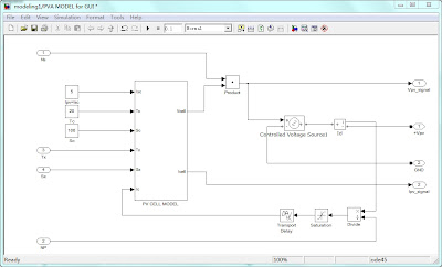
Today, we were tried to design the modeling
stage 2. The modeling stage 1 is a subsystem of the modeling stage 2 so this
stage should contain the block of stage 1. This stage is used to multiply the
cell voltage to form the full array voltage and then divide the array current by
the number of the cell in parallel to obtain the cell current. And solar cells
which we researched have 8 photovoltaic cells in series and only 1 line in
parallel. The block circuit is shown below:

In
this circuit, there are several new blocks used. This afternoon, we met our supervisor
Dr Tang to discuss the problems we encountered when we assigned value to these blocks
parameters. For the controlled voltage source is just used to change the input
value into voltage value so the parameter in this block doesn’t need to change.
For the Saturation part, only the current flow into this part, so the maximum
and minimum value of the current should the calculated. According to the voltage
equation, it can be found that the maximum value of current is 5.135 and the minimum
value of the current is 0. Then for the transport delay part, Mr Tang suggested
us to set the time delay to be 0.0001 so that enough test points can be got.

how can i find id symbol?
ReplyDeletewhat is the value for buffer size in transport delay ??
ReplyDelete